- 您现在的位置:买卖IC网 > Sheet目录3879 > PIC24F08KL401-I/SS (Microchip Technology)IC MCU 16BIT 8KB FLASH 20-SSOP
CHAPTER 4 PORT FUNCTIONS
User’s Manual U15905EJ2V1UD
140
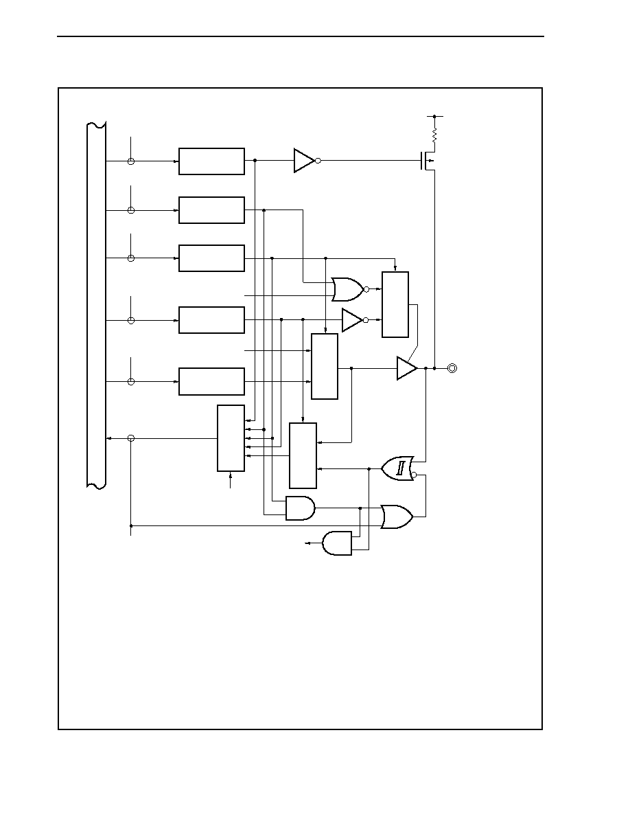
Figure 4-21. Block Diagram of P98, P910, and P913
Internal
bus
WRPMC
RD
Address
A8, A10, A13 output
RXD1, SI2, SI3 input
Output buffer
off signal
WRPORT
P98/A8/RXD1,
P910/A10/SI2,
P913/A13/SI3
PMC9n
Output latch
(P9n)
Selector
WRPU
PU9n
WRPM
PM9n
WRPFC
PFC9n
PMC9
P9
PU9
PM9
PFC9
EVDD
P-ch
Caution
These pins do not have hysteresis characteristics in the port mode.
They have hysteresis characteristics only when an input-pin alternate function is used.
Remarks 1. P9:
Port register 9
PM9:
Port mode register 9
PMC9: Port mode control register 9
PF9:
Port function register 9
PU9:
Pull-up resistor option register 9
Output buffer off signal: Signal that is active in the IDLE/STOP mode or during bus hold
2. n = 8, 10, 13
发布紧急采购,3分钟左右您将得到回复。
相关PDF资料
PIC16F689-I/SO
IC PIC MCU FLASH 4KX14 20SOIC
PIC16F689-I/ML
IC PIC MCU FLASH 4KX14 20QFN
PIC16F685-I/SO
IC PIC MCU FLASH 4KX14 20SOIC
PIC16F886-I/SO
IC PIC MCU FLASH 8KX14 28SOIC
PIC18LF6680T-I/L
IC PIC MCU FLASH 32KX16 68PLCC
PIC16C54C-20I/SS
IC MCU OTP 512X12 20SSOP
PIC16C621A-20/P
IC MCU OTP 1KX14 COMP 18DIP
PIC18F4439-E/P
IC PIC MCU FLASH 6KX16 40DIP
相关代理商/技术参数
PIC24F08KL401T-I/MQ
功能描述:16位微控制器 - MCU 8KB FLASH 1KB RAM 512B 3V 10-BIT ADC RoHS:否 制造商:Texas Instruments 核心:RISC 处理器系列:MSP430FR572x 数据总线宽度:16 bit 最大时钟频率:24 MHz 程序存储器大小:8 KB 数据 RAM 大小:1 KB 片上 ADC:Yes 工作电源电压:2 V to 3.6 V 工作温度范围:- 40 C to + 85 C 封装 / 箱体:VQFN-40 安装风格:SMD/SMT
PIC24F08KL401T-I/SO
功能描述:16位微控制器 - MCU 8KB FLASH 1KB RAM 512B 3V 10-BIT ADC RoHS:否 制造商:Texas Instruments 核心:RISC 处理器系列:MSP430FR572x 数据总线宽度:16 bit 最大时钟频率:24 MHz 程序存储器大小:8 KB 数据 RAM 大小:1 KB 片上 ADC:Yes 工作电源电压:2 V to 3.6 V 工作温度范围:- 40 C to + 85 C 封装 / 箱体:VQFN-40 安装风格:SMD/SMT
PIC24F08KL401T-I/SS
功能描述:16位微控制器 - MCU 8KB FLASH 1KB RAM 512B 3V 10-BIT ADC RoHS:否 制造商:Texas Instruments 核心:RISC 处理器系列:MSP430FR572x 数据总线宽度:16 bit 最大时钟频率:24 MHz 程序存储器大小:8 KB 数据 RAM 大小:1 KB 片上 ADC:Yes 工作电源电压:2 V to 3.6 V 工作温度范围:- 40 C to + 85 C 封装 / 箱体:VQFN-40 安装风格:SMD/SMT
PIC24F08KL402
制造商:MICROCHIP 制造商全称:Microchip Technology 功能描述:Low-Power, Low-Cost, General Purpose 16-Bit Flash Microcontrollers with nanoWatt XLP Technology
PIC24F08KL402-I/ML
功能描述:16位微控制器 - MCU 8KB FLASH 1KB RAM 512B 3V 10-BIT ADC RoHS:否 制造商:Texas Instruments 核心:RISC 处理器系列:MSP430FR572x 数据总线宽度:16 bit 最大时钟频率:24 MHz 程序存储器大小:8 KB 数据 RAM 大小:1 KB 片上 ADC:Yes 工作电源电压:2 V to 3.6 V 工作温度范围:- 40 C to + 85 C 封装 / 箱体:VQFN-40 安装风格:SMD/SMT
PIC24F08KL402-I/MQ
功能描述:16位微控制器 - MCU 8KB FL 1KB RAM 512B 3V 10-bit ADC RoHS:否 制造商:Texas Instruments 核心:RISC 处理器系列:MSP430FR572x 数据总线宽度:16 bit 最大时钟频率:24 MHz 程序存储器大小:8 KB 数据 RAM 大小:1 KB 片上 ADC:Yes 工作电源电压:2 V to 3.6 V 工作温度范围:- 40 C to + 85 C 封装 / 箱体:VQFN-40 安装风格:SMD/SMT
PIC24F08KL402-I/SO
功能描述:16位微控制器 - MCU 8KB FLASH 1KB RAM 512B 3V 10-BIT ADC RoHS:否 制造商:Texas Instruments 核心:RISC 处理器系列:MSP430FR572x 数据总线宽度:16 bit 最大时钟频率:24 MHz 程序存储器大小:8 KB 数据 RAM 大小:1 KB 片上 ADC:Yes 工作电源电压:2 V to 3.6 V 工作温度范围:- 40 C to + 85 C 封装 / 箱体:VQFN-40 安装风格:SMD/SMT
PIC24F08KL402-I/SP
功能描述:16位微控制器 - MCU 8KB FLASH 1KB RAM 512B 3V 10-BIT ADC RoHS:否 制造商:Texas Instruments 核心:RISC 处理器系列:MSP430FR572x 数据总线宽度:16 bit 最大时钟频率:24 MHz 程序存储器大小:8 KB 数据 RAM 大小:1 KB 片上 ADC:Yes 工作电源电压:2 V to 3.6 V 工作温度范围:- 40 C to + 85 C 封装 / 箱体:VQFN-40 安装风格:SMD/SMT